
HGLaser is a pioneer and leader in the application of lasers in China’s industrialization, leading globally in laser equipment and intelligent manufacturing solutions.
The company deeply understands the significant demand for transformation and upgrading in the industrial manufacturing field, providing overall solutions for intelligent manufacturing driven by technological innovation and intelligent interconnection.
Currently, the company’s products and solutions are widely used in many key sectors of the national economy such as consumer electronics, smart automobiles, semiconductors, engineering machinery, and rail transportation.
With forward-looking research and development, advantages in the entire industry chain, and a vast global service network, HGLaser can help you continuously breakthrough in the field of laser processing, ensuring worry free production.
LUV3220/LUV3320
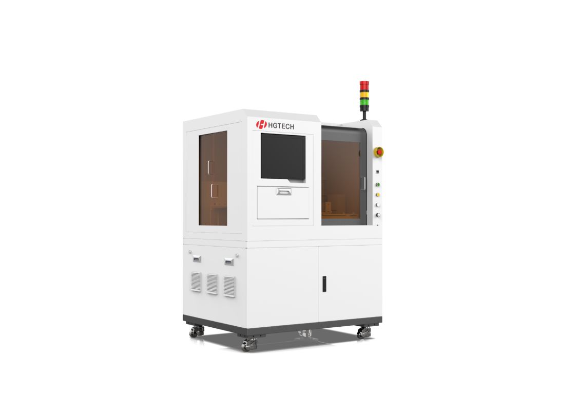
Mainly used for wafer marking, ID marking, utilizing customized lasers to perform localized processing on wafers. This process involves evaporating surface material to reveal deeper layers or inducing chemical and physical changes in surface material through light energy to “etch” traces, displaying various patterns, texts, barcodes, and other graphics required for etching on the wafer, serving the purpose of wafer traceability. It features high marking accuracy, fast speed, and clear marking.
LUA3200
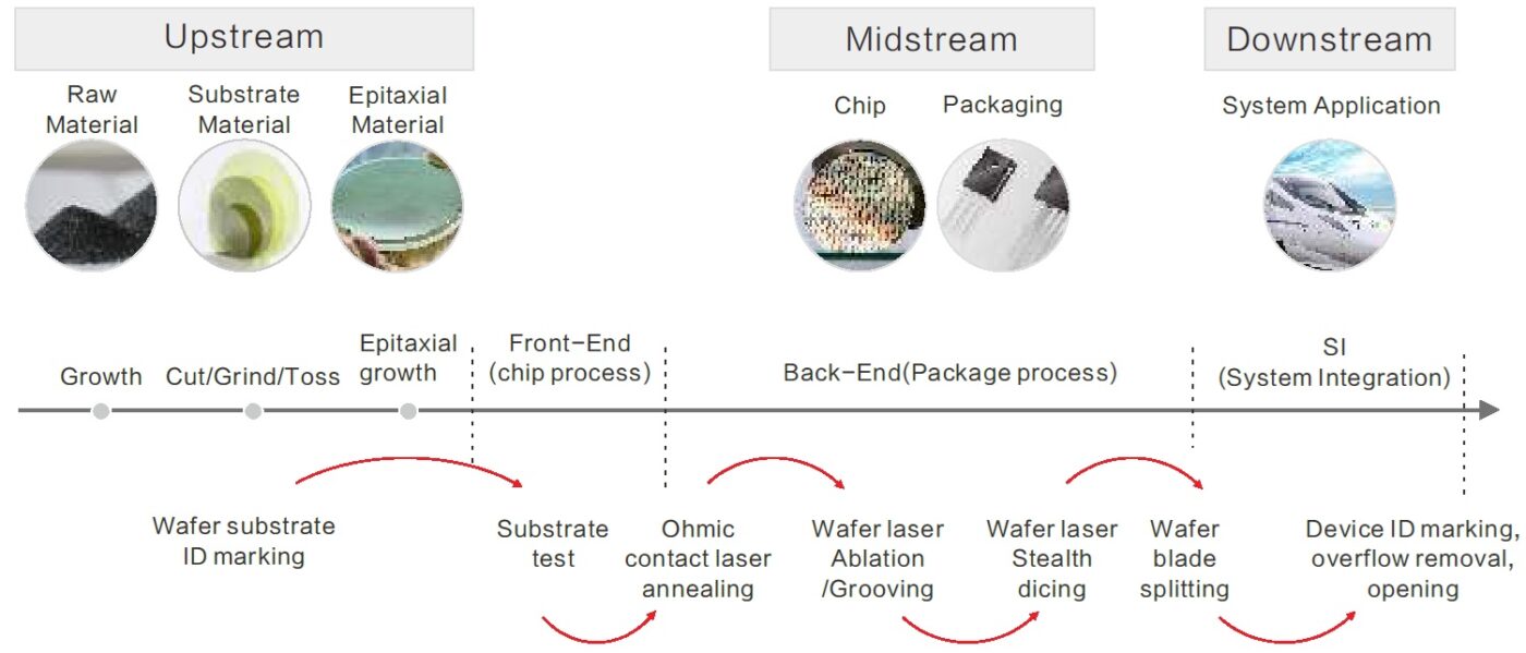
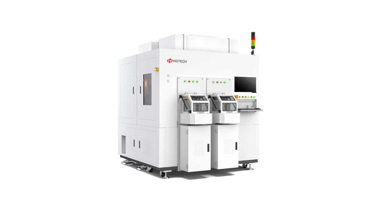
By utilizing the EFEM system for pre-alignment of the wafer, combined with customized laser annealing heads and relative motion of precision motion platforms, it achieves annealing of the backside metal (Ni or Ti layer) of the entire SiC wafer. This process forms a good ohmic contact, reducing contact resistance and improving device electrical performance.
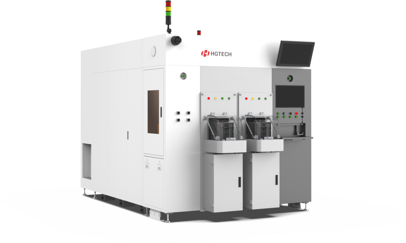
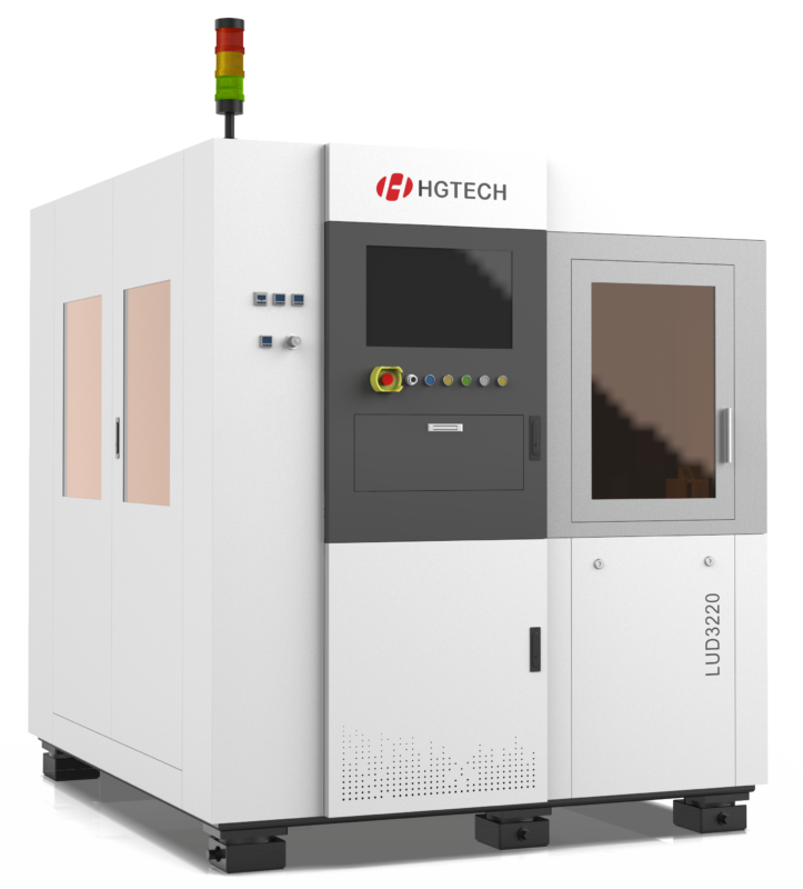
LUD3220
The fully automatic wafer laser cutting equipment utilizes multiple sets of high-precision CCD vision cameras to locate the entire wafer, enabling automatic identification and positioning of wafers with different grain specifications ranging from 6 to 8 inches. Combined with UV lasers and precision motion platforms for relative motion, it achieves surface ablation cutting (full cut, half cut, scribing, grooving) on the front/back side of the entire wafer.
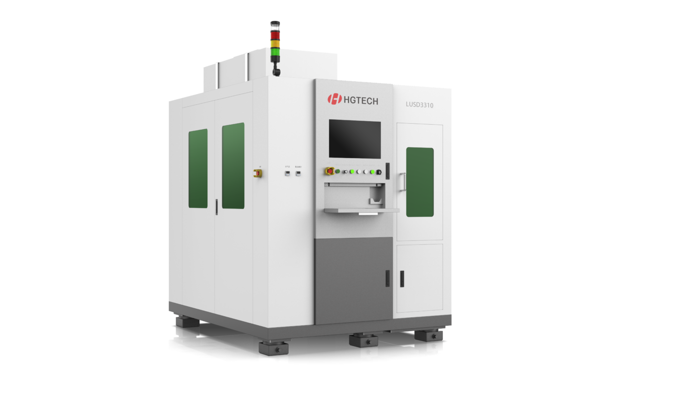
By utilizing multiple sets of high-precision CCD vision cameras, the entire wafer is accurately positioned, allowing for automatic identification and localization of wafers with different grain specifications ranging from 6 to 8 inches. This is combined with customized ultra-fast lasers and precision motion platforms to achieve relative
motion, enabling internal modification (hidden cutting) of the entire wafer. Subsequently, with the assistance of a dedicated wafer cleaving machine, the wafer is fully cleaved, and the chips are separated.
HUD3010
This product is primarily used for the wafer dicing process of SiC, Si, GaAs, ceramics, glass, and other wafers after laser cutting, facilitating high-precision
and high-efficiency separation of wafer grains.