SENTECH Instruments develops, manufactures, and sells worldwide advanced quality instrumentation for Plasma Etching, PECVD, Atomic Layer Deposition, Thin Film Measurement (Spectroscopic Ellipsometry, Spectroscopic Reflectometry and Laser Ellipsometer) and Photovoltaics.
Emphasize on low damage processing and non-invasive optical metrology.
Application laboratories are provided at SENTECH headquarters and Banner at different research institutes. At these locations, samples can be processed under optimal conditions. Each system can be demonstrated in operation. SENTECH has established an application network with universities and institutes offering access to leading edge technologies and processes for all our customers.
SENTECH plasma process equipment is manufactured under clean room conditions. Short assembling time, high throughput and clean environment are features that our customers appreciate.
SENTECH offers worldwide service supported by well-trained engineers in local markets. Short response time, qualifi ed technical support, and high reliability are key features of the SENTECH international service team.
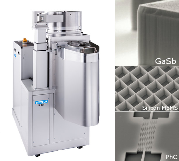
ICP-RIE plasma etcher
SI 500
Especially suited for low damage, high aspect ratio, high rate etching of semiconductors, dielectrics, and metals.
- Planar triple spiral antenna ICP source
- Dynamic substrate temperature control
- Helium backside cooling
- Mechanical clamping or e-chuck up to 200 mm wafer diameter
- Processing of single wafers and multiple wafers per carrier
- Wafer backside temperature measurement
- Cryogenic electrode
- Deep RIE extension
- Endpoint monitors (OES, SENTECH laser interferometer)
- Remote servicing
- SENTECH plasma tool software
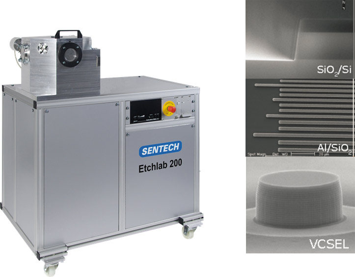
RIE plasma etcher
Etchlab 200, SI 591
Reactive Ion Etching (RIE) of dielectrics, metals, and Semiconductors.
- Direct load (Etchlab 200), load lock (SI 591)
- Capacitively coupled plasma source
- Shower head
- Substrate electrode for up to 8 inch wafer diameter
- Substrate temperature control between +10°C and +80°C
- Endpoint monitors (OES, SENTECH laser interferometer)
- Compact etchers with small footprint
- Remote servicing
- SENTECH plasma tool software
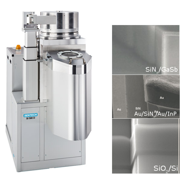
ICPECVD plasma deposition system
SI 500 D
Especially suited for low temperature and low damage deposition of SiO2, Si3N4, SiOxNy, SiC, a-Si, TEOS-SiO2. Film stress setting by process parameter control.
- Planar triple spiral antenna ICP source
- Dynamic substrate temperature control
- Helium backside cooling
- Mechanical clamping or e-chuck up to 200 mm wafer diameter
- Processing of single wafers and multiple wafers on carrier
- Biased substrate electrode
- Endpoint monitors (SENTECH laser interferometer)
- Remote servicing
- SENTECH plasma tool software
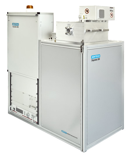
PECVD plasma deposition system
Depolab 200, SI 500 PPD
Deposition of dielectric films, SiC, amorphous silicon, TEOS.
- Direct load and load lock operation
- Capacitively coupled plasma source with shower head
- Low frequency mixing for stress control
- Integrated gas box
- Endpoint monitors (OES, SENTECH laser interferometer)
- Remote servicing
- Small footprint
- SENTECH plasma software
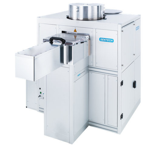
Plasma Enhanced Atomic Layer Deposition System
SILAYO
SENTECH atomic layer deposition systems enable thermal and plasma enhanced operation. The ALD systems can be configured for oxide, nitride, and metal deposition. 3D structures can be homogenously and conformally coated.
- PEALD with Planar Triple Spiral Antenna (PTSA) inductive coupled plasma source for best thin film uniformity < 1 %
- Sample size up to 330 mm diameter and 100mm height
- Stress control using RF bias
- High precision in thickness and composition control
- Smooth surfaces and sharp interfaces
- Stress control, especially for high thickness multilayers
- High uniformity and conformality on 3D shapes
- Reduced deposition temperatures for gentle processing
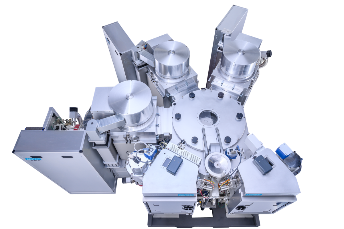
Cluster tools
- High throughput
- Processing without breaking the vacuum
- Process modules:
- ICP-RIE and RIE etch modules
- ICPECVD and PECVD deposition modules
- ALD module
- Transfer chambers: 3, 4, 6 port
- Fully automated wafer processing
- Vacuum cassette load lock
- Single wafer loading
Multi wafer processing
- 200, 300, and 380 mm carrier
- Carrier material: quartz, aluminum
- With and without He backside contact
- 2”, 3”, and 4” multi wafer processing
- ICP-RIE and ICPECVD systems with 300 mm electrode and load lock
- RIE and PECVD systems with 380 mm electrode and manual loading
DUV-VIS-NIR
spectroscopic ellipsometer
SENresearch 4.0
Large variety of options for R & D and routine applications from DUV to NIR.
- Widest spectral range 190 nm (deep UV) – 3,500 nm (NIR)
- No moving parts with SSA principle
- Full Mueller matrix by innovative 2 C design
- SpectraRay/4 comprehensive ellipsometry software
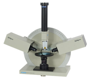
Cost-effective ellipsometer SENpro
Focused on speed and accuracy for the measurement of thin films (1 nm to 15 μm).
- Spectral range 370 –1,050 nm
- Goniometer with preset angles of incidence
- Step Scan Analyzer principle for highest measurement accuracy
- Spectroscopic ellipsometer software SpectraRay/4
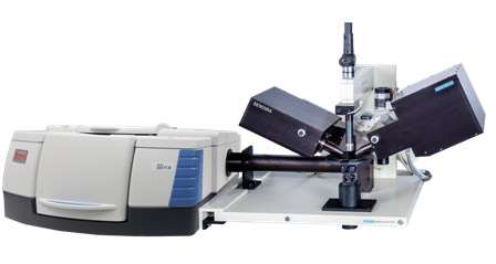
Infrared spectroscopic ellipsometer
SENDIRA
Vibrational spectroscopic analysis of thin layers (dielectric layers, TCOs, semiconductors, organic layers).
- IR spectral range 1,700 – 25,000 nm
- Fully applicable FTIR spectrometer
- Proprietary ellipsometer software SpectraRay/4
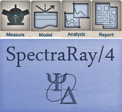
Spectroscopic ellipsometer software
SpectraRay/4
User-friendly software with recipe oriented mode for operators and advanced mode for interactive measurement and modeling.
- Supports variable angle, multiexperiment, and combined
photometric measurements - Ellipsometric, reflection, and transmission data
- Huge library of materials‘ data, large number of dispersion models
- Sample effects: depolarization, non-uniformity, scattering
(Muellermatrix), backside reflection
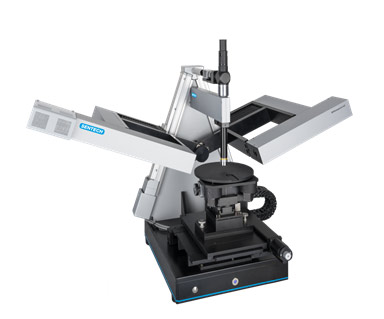
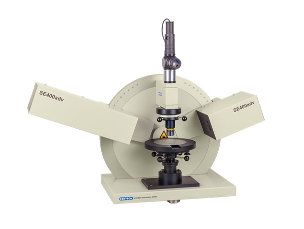
Multiple angle laser ellipsometer
SE 400adv
Characterization of single films and substrates in microelectronic, photovoltaic, data storage, display technology, life science, metal processing, etc.
- Application specific angles of incidence
- HeNe laser of 632.8 nm wavelength
- Measurement precision of 0.1 Å
- High measurement speed allows for film growth monitoring and endpoint detection
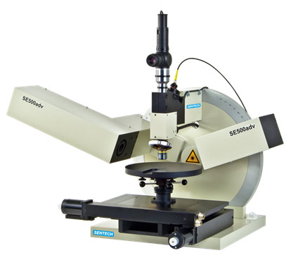
Combined Ellipsometry Refl ectometry
SE 500adv
Maximum flexibility for the analysis of thick dielectric, organic, photoresist, silicon, or polysilicon films.
- Fast and unambiguous determination of the thickness of transparent films up to 25 μm
- Multiple angle manual goniometer for the characterization of single films and layer stacks
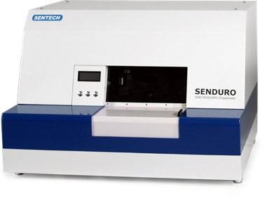
Automated ellipsometer for R & D
SENDURO
Fast, highly precise, and repeatable measurements in production, process monitoring, and R & D.
- Spectral range 290 – 850 nm
- Patented automatic alignment sensors
- Step Scan Analyzer principle for highest measurement accuracy
- Small footprint
- Routine applications
- Proprietary ellipsometer software SpectraRay/4
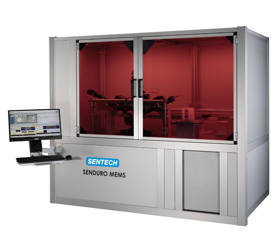
Ellipsometer for routine applications
SENDURO® MEMS
Very fast measurement of films between a few ångstrom and more than 50 μm thickness.
- Cassette loading up to 8″ wafers
- Spectral range 290 – 850 nm
- Recipe based measurements
- Proprietary ellipsometer software SpectraRay/4
- Up to 80 μm spot size
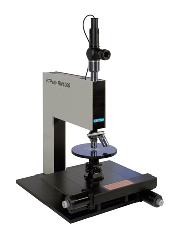
Spectroscopic reflectometer
RM 1000 / 2000
Accurate measurements of reflectance, film thickness, and optical constants of films between 5 nm and 50 μm.
- Small spot size
- UV to NIR spectral range
- Most accurate measurement by height and tilt adjustment of samples
- Optional high resolution mapping
- Comprehensive, recipe-oriented reflectometer software FTPadv EXPERT
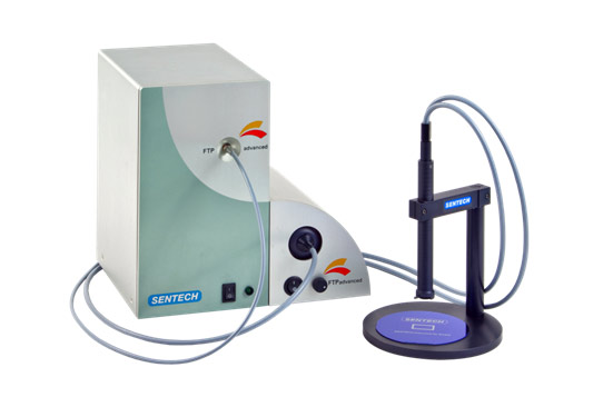
Film Thickness Probe
FTPadv
Fast and easy measurement of film thickness in production, process monitoring, and R & D.
- Thickness range 30 nm – 25 μm
- Recipe oriented software
- Adaptation to a microscope for measurements in small areas