EV Group (EVG) targets advanced packaging, compound semiconductor and silicon-based power devices, MEMS, nanotechnology and SOI markets with its industry-leading wafer-bonding, lithography/nanoimprint lithography(NIL), metrology, photoresist coating, cleaning and inspection equipment.
EV Group holds the dominant share of the market for wafer bonding equipment (especially SOI bonding) and is a leader in lithography for advanced packaging and nanotechnology.
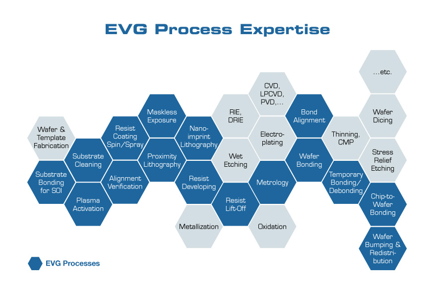
EVG’s comprehensive process knowledge is a result of decades of experience and creates benefits and advantages for our customers, from development to production.
With state-of-the-art application labs based at its headquarters in Austria, along within the U.S. and Japan, EV Group is focused on delivering superior process expertise to its growing global customer base every step of the way, be it from initial development through final integration at the customer’s site.
For nearly 40 years, EVG has provided industry-leading process technologies and solutions that have enabled innovations in advanced packaging, optics and photonics, sensors and bio-medical devices and applications.


EV Group offers a complete portfolio of wafer-level manufacturing solutions for various micro- and nanotechnology applications and products, addressing established as well as emerging markets. Our field-proven equipment, combined with EV Group’s superior process expertise and development support, enable our global customer base to stay one step ahead of the competition.


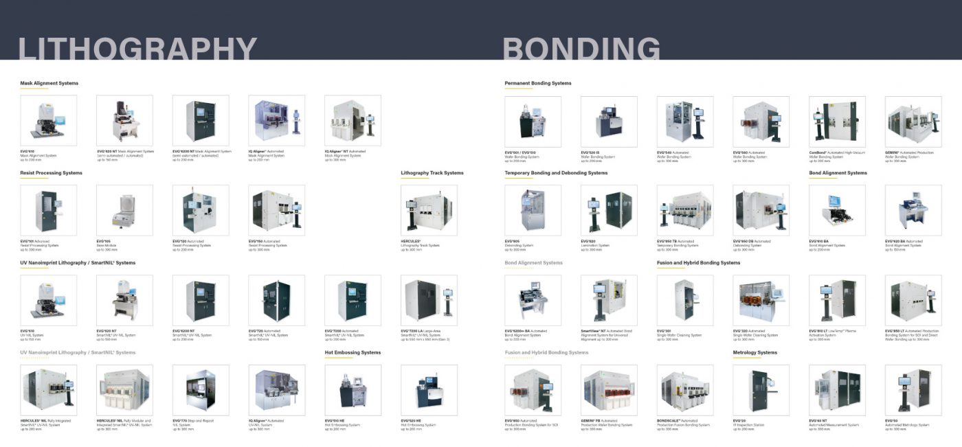
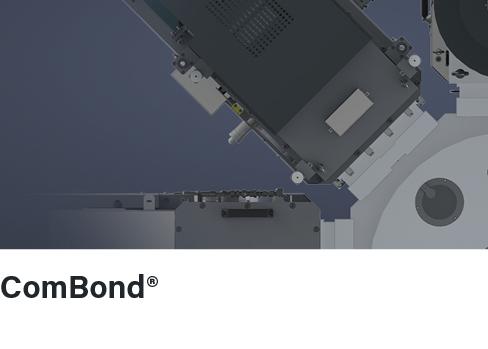
The basis for EVG’s success is their products: lithography, bonding and imprint systems. Below showcasing some of the systems offered by EVG.