3D-Micromac is the leading specialist in laser micromachining. The team of experts develop processes, machinery and complete systems at the highest technical and technological level.
3D-Micromac systems have been successfully implemented in various high-tech industries worldwide including photovoltaic, semiconductor, glass and display industries, micro diagnostics, and medical technology.
3D-Micromac’s target is to completely satisfy customer demands even on the most complex projects.
3D-Micromac adheres to high-performance and future-oriented processes at high production efficiency. Setting international standards for true innovation with their technologies.
Since placing great importance on continually expanding their know-how, 3D Micromac is diligent about keeping up with the latest research. On a daily basis, 3D Micromac combine recent results with customers’ demands to realize them in practise
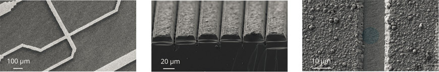
Laser Structuring and Selective Ablation
Lasers are, based on the outstanding ability to narrowly focus them, capable of extremely precisely and even selectively ablate materials from metals, ceramics, polymers or multilayer stacks.
Laser machining offers a unique and digital option to achieve maximum quality and precision whilst guaranteeing highest efficiency and throughput. Selective as well as contactless material ablation are very important for defined processes.
Machining in this range is preferably done with short pulsed or ultra short pulsed lasers. A prerequisite for the effective implementation of laser structuring is the use of a laser source with optimal beam quality at very high output powers and pulse repetition rates. These laser sources allow for the generation of smallest possible micro patterns in the range of a few micrometers, the fabrication of 3D objects, and the selective ablation of functional layers and coatings.
These technologies are utilized in different fields of application, such as:
- Surface modification in medical device technology and microfluidics
- Scribing and patterning in semiconductor and photovoltaics industry
- removal of layers and coatings, e.g. ITO/TCO, on flexible electronic components including LED, µLED and OLED technologies
- 2D or 3D structuring
- Laser micro engravings.
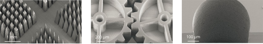
Laser precision drilling enables generation of microholes with well-defined geometries
The drilling of microholes with well-defined geometries is gaining significance in a wide variety of industries. Laser drilling in turn is replacing conventional drilling processes to support many applications, ranging from the setting of micro-drillings in throughput flow filters and sieves, to via drillings in high-performance solar cells, and injection jets in the automotive industry. Laser techniques are gaining ground in the production of printer inkjets due to the laser’s touch-less processing, precise dosing of energy input, minimal heat transmission into the material, precision, and repeatability. Laser techniques also provide additional flexibility in defining the drilling geometries. For example, it is possible to generate microholes with a high aspect ratio (the relation between the drilling depth and the drilling diameter) or microholes with defined taper by varying the machining strategy during the laser process.
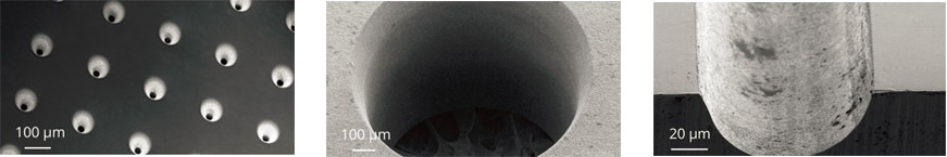
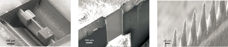
Unrivaled Laser Processing Technology for the Generation of Free-Form Geometries in Glass and Sapphire
For producing straight, cylindrical holes or undercut geometries in transparent materials, 3D-Micromac has developed the so-called FSLA™ process (Flow Supported Laser Ablation). This patent pending ablation method involves the use of an ultrashort pulse laser. Typical used pulse durations are less than 20ps. The material is processed from the back side while the focus level is fed in the material (continuous or discrete focus steps) while ablation. An associated defined flow is streamed against the back of the substrate during the entire laser process.
This stream is adapted precisely to the ablation process, and transports away the debris of the ablation process as well as helps prevent heat from accumulating in the substrate. Flow media and additives may vary with application. Flow volume as well as pressure need to be adapted to laser settings. Well aligned settings allow to process material thicknesses between 50 µm and 50 mm in this manner.
There is an increasing demand for preparation techniques tuned to manifold methods of microstructure diagnostics that need to be fast, reliable, cost effective, artifact-free, and targeted. Besides traditional mechanical sample preparation, focused-ion-beam micromachining is currently dominating the field. While the former is accompanied by high costs for skilled personnel, the latter is characterized by very high costs of ownership.
Laser-based sample preparation represents a very valuable alternative approach. Based on patented processes, the microPREP™ is ready to prepare samples for TEM, X-SEM, APT, and micromechanical testing in an almost entirely automated fashion. Making use of a rugged pulsed laser source, the process is characterized by very low running costs, suitability for semiconductors, metals, ceramics, as well as compounds thereof, and a very high targeted precision on the micron scale.
Enabling Technology for Fast, Clean, and Cost-Effective Wafer Dicing
TLS-Dicing™ (Thermal Laser Separation) is a unique technology for separating wafers into single chips in semiconductor back-end processing. TLS-Dicing™ uses thermally induced mechanical stress to separate brittle semiconductor materials, like silicon (Si) and silicon carbide (SiC) wafers.
TLS-Dicing™ is an ideal solution for wafer dicing that has many advantages compared to competing technologies, such as the currently established method of mechanical sawing as well as laser ablation. These include:
- High separation speed: 300 mm/s
- Very smooth edges (reduces leakage current of diodes)
- Clean and nearly dry process
- Nearly no chipping and micro cracks for less breakage
- Thin back side metal can be separated without damage
- No tool wear
- Lower cost of ownership due to no tool wear and nearly no consumables
- Zero Kerf cleaving process for reduced street width, enabling more die per wafer
- Applicable to larger diameter substrates (e.g. 300 mm)
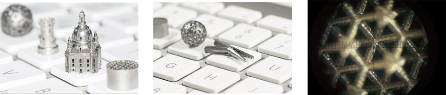
Additive Manufacturing of Micro Metal Parts
Laser Sintering is additive manufacturing technology, also known as 3D Printing, Selective Laser Sintering, and Selective Laser Melting. With Micro Laser Sintering, we merge the advantages of additive manufacturing and micro machining for the first time to generate complex micro metal parts of incredible accuracy, detail resolution and surface quality. The technology offers highest flexibility in manfacturing process, low operating costs, and user-friendliness.
With Micro Laser Sintering it is possible to process nonreactive and reactive materials, e.g. stainless steel, molybdenum, tungsten, titanium, and gold. The combination of a very small laser beam spot size and a unique micro metal powder allows the generation of micro parts with super thin layers and a very high part density. These advantages result in the ability to manufacture moveable parts and assemblies in a single step.
Micro Laser Sintering is ideally suited to manufacture micro metal parts for medical device industry, semiconductor industry, aerospace, as well as jewelry and watchmaking.
The Micro Laser Sintering technology has been developed and is continuously improved by 3D MicroPrint GmbH.