Diener Electronic is an innovative company in the field of plasma technology and an international leader in the production of low-pressure plasma systems, plasma HF generators and atmospheric plasma. Their technological maturity and resounding success guarantee continuous, global expansion.
Till date, there are already more than 10,000 Diener Plasma systems worldwide!
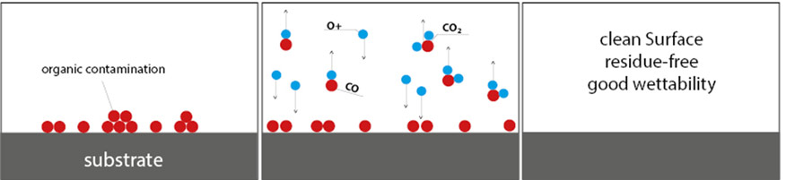
Organic residue can be found on even the cleanest surfaces. Release agent residue is present on components that have just rolled off the production line, and even short-term exposure to the surrounding air leads to deposits from the atmosphere. Wet chemical cleaning will not remove these deposits from cavities and narrow gaps. Moreover, it pollutes the environment and often damages the substrate itself. Plasma cleaning removes all organic residue from any material.
- For all surfaces that need coatings, adhesive bonds, paint finishes or ink patterns to adhere.
- Low-pressure plasma does not harm the substrate chemically or thermally. As a result, practically any solid materials can be cleaned in plasma.
- All those who require high-quality connections, adhesive bonds, coatings, ink patterns or paint finishes.
- Micro-sandblasting can remove any inorganic residues that is hard to remove by other means. Bombardment with high-energy argon ions can be used on any coating (non-selective).
- Perfect adhesion and perfect electrical contact require clean metal surfaces. Plasma treatment removes oxide layers.
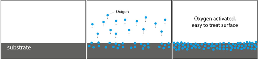
Even perfectly clean surfaces can have poor adhesive qualities due to a material’s low surface energy. Non-polar plastics, in particular bulk plastics like PP, PE, POM, are affected the most. Plasma treatment in oxygen or air plasma creates polar binding sites and increases the surface energy.
- For all substrates with poor adhesion properties to be bonded, coated, painted or printed on.
- Finishing of plastic components.
- Creates an adhesive bond on components which could not be connected previously.
- Plasma activation makes it possible to bond any material, even PTFE
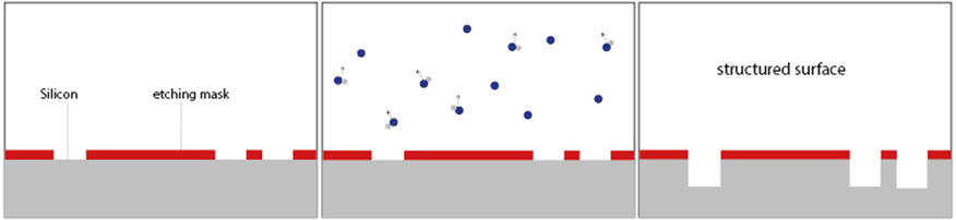
Plasma technology makes anisotropic and isotropic etching possible: Isotropic etching by means of chemical multi directional etching, anisotropic etching by means of physical etching (ion etching approach the surface approx. from one direction), as well as (RIE = Reactive IonEtching).
Isotropic etching is made possible by polymeric degradation and chemical reaction on organic materials.
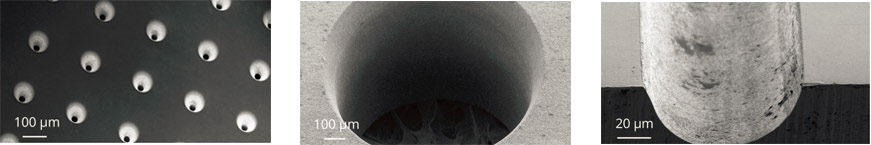
- Nanostructuring of surfaces for surface enlargement and improved adhesion.
- Etching of PTFE
- For perfect paint and glue adhesion when dealing with difficult connection problems.
- Good bio-integration of implants.
- Photoresist ashing.
- Removal of oxide layers.
- Filter ashing for asbestos analysis.
Anisotropic etching by ion bombardment is generally effective on any substrate.
- Etching masks for printed circuit boards.
- Micro-fluidic structures Photolithographic production of PDMS chips and bonding (LOC = Lab On-Chip).
- Micro-mechanical components.
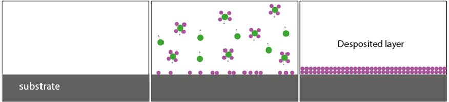
There are various coating methods based on low-pressure plasma:
- CVD (Chemical Vapour Deposition).
- DLC (Diamond Like Carbon).
- Plasma sputtering.
- Plasma polymerisation.
The method of plasma polymerisation is of particular importance. Monomer gases, which are used as process gases, react to polymers in the plasma and are then deposited on the substrate as a solid layer. With this method firmly adhering PTFE-like coatings can be produced.
- Depositing hydrophobic layers.
- Depositing hydrophilic layers.
- Depositing protective or insulating layers.
- May be used as a diffusion barrier, for example
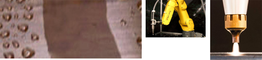
A gas discharge is ignited between a central electrode and an insulated ring electrode. A plasma is excited in the stream of gas flowing through. The plasma is blown out through the nozzle.
There is no high voltage in the plasma jet. Metallic substrates can also be treated. The temperature is relatively high. Thermally sensitive substrates can only be treated very briefly in a continuous manner.
The effective treatment spot has a diameter of approx. 10-12 millimetre, but treatment speed is high. The plasma can therefore generally be guided over the substrate quickly.
The effective treatment spot has a diameter of approx. 10-12 millimetre, but treatment speed is high. The plasma can therefore generally be guided over the substrate quickly.
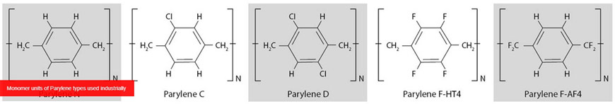
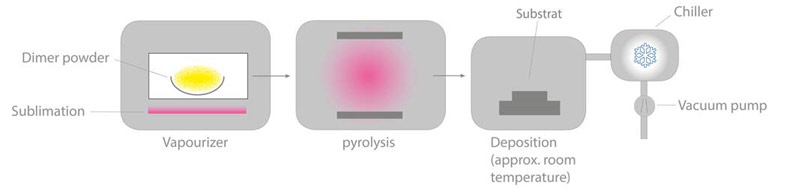
Parylene are derivatives of benzene. The basic form of Parylene N consists of a benzene molecule. At the benzene ring, at two corners, each hydrogen atom is replaced by a CH2 group. The prefix “para” (abbreviated “p”) indicates that these two CH2 groups are attached to the opposite corners of the benzene hexagon.
Parylene coating machines are basically vacuum systems. Thus, they include in each case a vacuum‑tight and pressure‑tight vacuum chamber and a vacuum pump. With approximately 0.02 -0.1 mbar, the working pressure is not particularly low. To obtain a good layer quality, it is desirable that foreign molecules are removed as far as possible.
High quality seals, avoidence of out-gassing from components and a powerful vacuum pump, are necessary to reach good coating conditions.
The unique properties of Parylene:
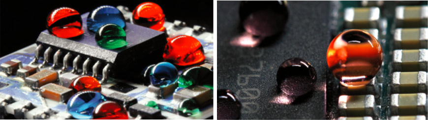
- Constant coating thickness, independent of the substrate geometry.
- Pinhole-free, starting from 1 micron.
- Extraordinary good penetration in crevices and holes.
- Very good barrier properties (especially for parylene C).
- Insolubility.
- Food Authenticity and biocompatibility.
- No environmental impact.
- High temperature resistance (Parylene F-AF4).
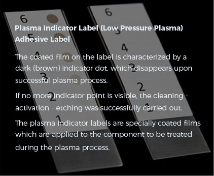
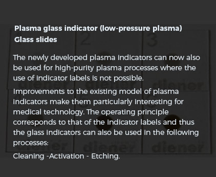
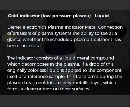
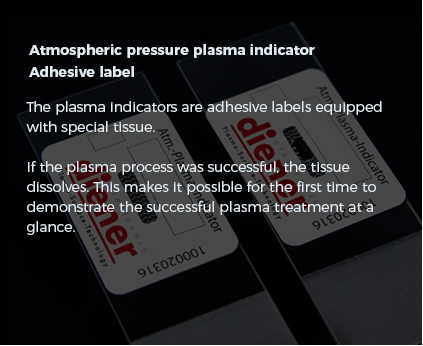
Plasma indicators are simple and fast test methods for the detection of successful plasma processes.
If component surfaces do not have the desired properties after plasma treatment, expensive complaints can quickly ensue.
However, there are simple procedures that can be used to demonstrate a successful plasma process without much time.